- 您现在的位置:买卖IC网 > Sheet目录471 > MAX19998ETP+ (Maxim Integrated)IC MIXER DOWNCONVERSION 20TQFN
SiGe, High-Linearity, 2300MHz to 4000MHz
Downconversion Mixer with LO Buffer
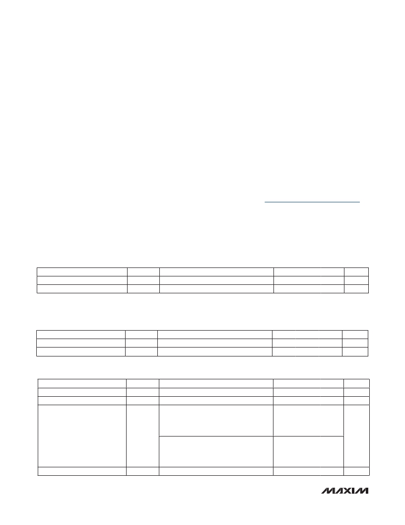
ABSOLUTE MAXIMUM RATINGS
V CC to GND..........................................................-0.3V to +5.5V
IF+, IF-, LOBIAS, IFBIAS to GND ............. -0.3V to (V CC + 0.3V)
RF, LO Input Power ....................................................... +12dBm
RF, LO Current
(RF and LO is DC shorted to GND through balun) ........50mA
Continuous Power Dissipation (Note 1) .................................5W
B JA (Notes 2, 3) ............................................................ +38 N C/W
B JC (Notes 1, 3) ............................................................ +13 N C/W
Operating Case Temperature Range
(Note 4).................................................. T C = -40 N C to +85 N C
Junction Temperature .....................................................+150 N C
Storage Temperature Range............................ -65 N C to +150 N C
Lead Temperature (soldering, 10s) ................................+300 N C
Note 1: Based on junction temperature T J = T C + ( B JC x V CC x I CC ). This formula can be used when the temperature of the
exposed pad is known while the device is soldered down to a PCB. See the Applications Information section for details.
The junction temperature must not exceed +150 N C.
Note 2: Junction temperature T J = T A + ( B JA x V CC x I CC ). This formula can be used when the ambient temperature of the PCB is
known. The junction temperature must not exceed +150 N C.
Note 3: Package thermal resistances were obtained using the method described in JEDEC specification JESD51-7, using a four-
layer board. For detailed information on package thermal considerations, refer to www.maxim-ic.com/thermal-tutorial .
Note 4: T C is the temperature on the exposed pad of the package. T A is the ambient temperature of the device and PCB.
Stresses beyond those listed under “Absolute Maximum Ratings” may cause permanent damage to the device. These are stress ratings only, and functional
operation of the device at these or any other conditions beyond those indicated in the operational sections of the specifications is not implied. Exposure to absolute
maximum rating conditions for extended periods may affect device reliability.
5.0V SUPPLY DC ELECTRICAL CHARACTERISTICS
(Typical Application Circuit, R1 = 698 ω , R2 = 604 ω, V CC = 4.75V to 5.25V, no input RF or LO signals. T C = -40 N C to +85 N C, unless
otherwise noted. Typical values are at V CC = 5.0V, T C = +25 N C, all parameters are production tested.)
PARAMETER
SYMBOL
CONDITIONS
MIN
TYP
MAX
UNITS
Supply Voltage
Supply Current
V CC
I CC
Total supply current
4.75
5.0
230
5.25
247
V
mA
3.3V SUPPLY DC ELECTRICAL CHARACTERISTICS
(Typical Application Circuit , R1 = 845 ω , R2 = 1.1k ω, V CC = 3.0V to 3.6V, no input RF or LO signals. T C = -40 N C to +85 N C, unless oth-
erwise noted. Typical values are at V CC = 3.3V, T C = +25 N C, parameters are guaranteed by design, unless otherwise noted.) (Note 5)
PARAMETER
Supply Voltage
Supply Current
SYMBOL
V CC
I CC
CONDITIONS
Total supply current
MIN
3.0
TYP
3.3
150
MAX
3.6
UNITS
V
mA
RECOMMENDED AC OPERATING CONDITIONS
PARAMETER
RF Frequency Range
LO Frequency
SYMBOL
f RF
f LO
(Notes 5, 6)
(Notes 5, 6)
CONDITIONS
MIN
2300
2600
TYP
MAX
4000
4300
UNITS
MHz
MHz
Using a Mini-Circuits TC4-1W-17 4:1
transformer as defined in the Typical
Application Circuit , IF matching components
100
500
IF Frequency
f IF
affect the IF frequency range (Notes 5, 6)
Using a Mini-Circuits TC4-1W-7A 4:1
transformer as defined in the Typical
Application Circuit , IF matching components
50
250
MHz
affect the IF frequency range (Notes 5, 6)
LO Drive
P LO
-3
0
+3
dBm
2
______________________________________________________________________________________
发布紧急采购,3分钟左右您将得到回复。
相关PDF资料
MAX19999ETX+T
IC DOWNCONVERTER 2CH 36TQFN
MAX2009ETI+T
IC RF PREDISTORT ADJ 28-TQFN
MAX2010ETI+T
IC RF PREDISTORT ADJ 28-TQFN
MAX2014ETA+T
IC DETECT/CNTRL LOG 8-TDFN
MAX2015EUA+T
IC DETECT/CNTRL LOG 8-UMAX
MAX2015EVKIT
EVAL KIT FOR MAX2015
MAX2016ETI+T
IC DETECT/CNTRL LOG 28-TQFN
MAX2021ETX+T
IC MOD/DEMOD 36-TQFN
相关代理商/技术参数
MAX19998ETP+T
功能描述:上下转换器 High-Gain 2.3GHz to 4.5GHz Downconv RoHS:否 制造商:Texas Instruments 产品:Down Converters 射频:52 MHz to 78 MHz 中频:300 MHz LO频率: 功率增益: P1dB: 工作电源电压:1.8 V, 3.3 V 工作电源电流:120 mA 最大功率耗散:1 W 最大工作温度:+ 85 C 安装风格:SMD/SMT 封装 / 箱体:PQFP-128
MAX19998EVKIT#
制造商:Maxim Integrated Products 功能描述:SIGE HIGH-LINEARITY 2300MHZ TO 4000MHZ DOWNCONVERSION MIXER - Boxed Product (Development Kits)
MAX19999A
功能描述:上下转换器
RoHS:否 制造商:Texas Instruments 产品:Down Converters 射频:52 MHz to 78 MHz 中频:300 MHz LO频率: 功率增益: P1dB: 工作电源电压:1.8 V, 3.3 V 工作电源电流:120 mA 最大功率耗散:1 W 最大工作温度:+ 85 C 安装风格:SMD/SMT 封装 / 箱体:PQFP-128
MAX19999ETX+
功能描述:上下转换器 High-Gain 3GHz to 4GHz Downconv RoHS:否 制造商:Texas Instruments 产品:Down Converters 射频:52 MHz to 78 MHz 中频:300 MHz LO频率: 功率增益: P1dB: 工作电源电压:1.8 V, 3.3 V 工作电源电流:120 mA 最大功率耗散:1 W 最大工作温度:+ 85 C 安装风格:SMD/SMT 封装 / 箱体:PQFP-128
MAX19999ETX+T
功能描述:上下转换器 High-Gain 3GHz to 4GHz Downconv RoHS:否 制造商:Texas Instruments 产品:Down Converters 射频:52 MHz to 78 MHz 中频:300 MHz LO频率: 功率增益: P1dB: 工作电源电压:1.8 V, 3.3 V 工作电源电流:120 mA 最大功率耗散:1 W 最大工作温度:+ 85 C 安装风格:SMD/SMT 封装 / 箱体:PQFP-128
MAX1999EEI
功能描述:DC/DC 开关控制器 RoHS:否 制造商:Texas Instruments 输入电压:6 V to 100 V 开关频率: 输出电压:1.215 V to 80 V 输出电流:3.5 A 输出端数量:1 最大工作温度:+ 125 C 安装风格: 封装 / 箱体:CPAK
MAX1999EEI+
功能描述:DC/DC 开关控制器 Quad Out Main Power Supply Controller RoHS:否 制造商:Texas Instruments 输入电压:6 V to 100 V 开关频率: 输出电压:1.215 V to 80 V 输出电流:3.5 A 输出端数量:1 最大工作温度:+ 125 C 安装风格: 封装 / 箱体:CPAK
MAX1999EEI+T
功能描述:DC/DC 开关控制器 Quad Out Main Power Supply Controller RoHS:否 制造商:Texas Instruments 输入电压:6 V to 100 V 开关频率: 输出电压:1.215 V to 80 V 输出电流:3.5 A 输出端数量:1 最大工作温度:+ 125 C 安装风格: 封装 / 箱体:CPAK
